Modulation doping in semiconductor nanostructures
To date, considerable efforts have been made to improve the transport properties (e.g., high carrier mobility and transconductance) of (doped) crystalline SiNWs or silicon nanotubes (SiNTs) for the future electronic and photonic device applications. For the general doping technique used in crystalline SiNWs or SiNTs, however, significant backscattering induced by ionized impurities will present while increasing the carrier concentration, which then reduces the charge transmission for conducting channels. This motivates us to explore methods to reduce the impurity scattering in these nanodevices.
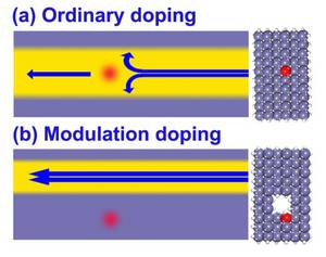
Schematic of impurity scattering in (a) ordinary doping and (b) modulation doping. The conduction channel is indicated by yellow color and the carrier transport is showed by blue arrows. The dopant is represented by red point. Their corresponding structure models are shown on the right as examples, where cyan, white and red balls represent for Si, H and impurity (e.g. B or P) atoms, respectively.
On the other hand, our first-principles calculations of SiNTs show a unique quantum confinement behavior: the electronic wave functions of the valence band maximum(VBM) and conduction band minimum(VBM) are due mainly to atoms located in the thicker side of the tube wall. This is advantageous to spatially separate the doping impurities from the conducting channel in doped SiNTs. It was pointed out that the performance of the SiNT-based transistors may be substantially improved by selective p/n doping in the thinner side of the tube wall in the spirit of modulation doping. From the nonuniform distributions of the VBM and CBM caused by quantum confinement, we expect that this kind of modulation doping can be applied to other semiconductor nanostructures whose confined length is comparable to or less than the corresponding Bohr exciton radius (e.g. ~ 4.9 nm for Si ). Compared with the conventional modulation doping, our method does not depend on a heterostructure, and thereafter, the complication in transistor technology and the scattering by interface can be effectively avoided.
We will study the quantum confinement, electronic and transport properties of low dimensional semiconductor nanostructures: nanotubes, nanowires, and thin films with nonuniform thickness. The modulation doping idea will be applied to those structures and their transport properties will be calculated to estimate quantitatively the superiority of our doping method. We will simulate large systems wtih thousands of atoms which is more practical in experiments and aim to design nano-devices of high conductance and high carrier density.
Selected publications
Posters
Investigators
Dr. Binghai Yan
Dr. Andreia da Rosa
Dr. Thomas Niehaus
Support
Alexander von Humboldt Foundation of Germany
Collaborations
Prof. Wenhui Duan
Tsinghua University , Beijing, China